- 您现在的位置:买卖IC网 > Sheet目录3821 > PIC18F2620-I/SO (Microchip Technology)IC MCU FLASH 32KX16 28SOIC
PIC18F2525/2620/4525/4620
DS39626E-page 24
2008 Microchip Technology Inc.
TABLE 2-2:
CAPACITOR SELECTION FOR
CRYSTAL OSCILLATOR
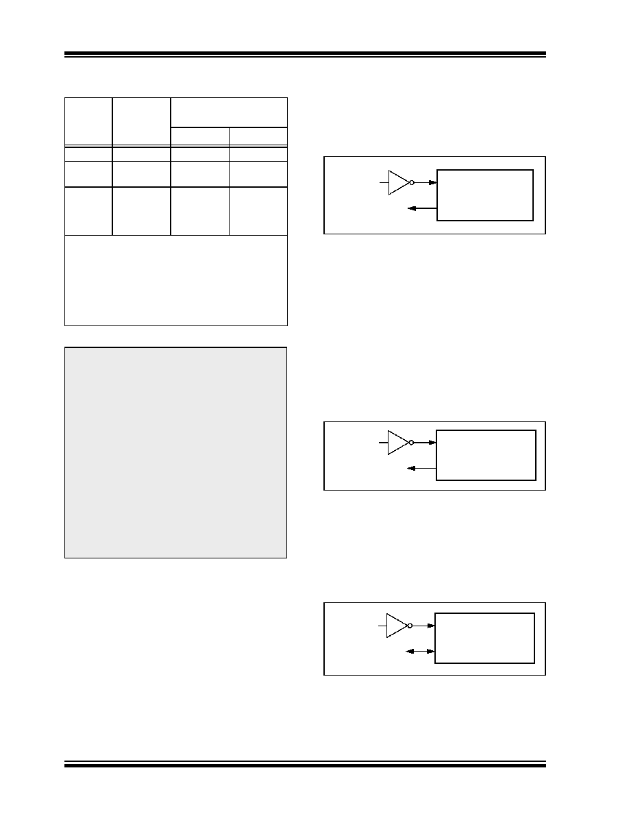
An external clock source may also be connected to the
OSC1 pin in the HS mode, as shown in Figure 2-2.
FIGURE 2-2:
EXTERNAL CLOCK
INPUT OPERATION
(HS OSCILLATOR
CONFIGURATION)
2.3
External Clock Input
The EC and ECIO Oscillator modes require an external
clock source to be connected to the OSC1 pin. There is
no oscillator start-up time required after a Power-on
Reset or after an exit from Sleep mode.
In the EC Oscillator mode, the oscillator frequency
divided by 4 is available on the OSC2 pin. This signal
may be used for test purposes or to synchronize other
logic. Figure 2-3 shows the pin connections for the EC
Oscillator mode.
FIGURE 2-3:
EXTERNAL CLOCK
INPUT OPERATION
(EC CONFIGURATION)
The ECIO Oscillator mode functions like the EC mode,
except that the OSC2 pin becomes an additional
general purpose I/O pin. The I/O pin becomes bit 6 of
PORTA (RA6). Figure 2-4 shows the pin connections
for the ECIO Oscillator mode.
FIGURE 2-4:
EXTERNAL CLOCK
INPUT OPERATION
(ECIO CONFIGURATION)
Osc Type
Crystal
Freq
Typical Capacitor Values
Tested:
C1
C2
LP
32 kHz
30 pF
XT
1 MHz
4 MHz
15 pF
HS
4 MHz
10 MHz
20 MHz
25 MHz
15 pF
Capacitor values are for design guidance only.
Different capacitor values may be required to produce
acceptable oscillator operation. The user should test
the performance of the oscillator over the expected
VDD and temperature range for the application.
See the notes following this table for additional
information.
Note 1: Higher capacitance increases the stability
of the oscillator but also increases the
start-up time.
2: When operating below 3V VDD, or when
using certain ceramic resonators at any
voltage, it may be necessary to use the
HS mode or switch to a crystal oscillator.
3: Since each resonator/crystal has its own
characteristics, the user should consult
the resonator/crystal manufacturer for
appropriate
values
of
external
components.
4: Rs may be required to avoid overdriving
crystals with low drive level specification.
5: Always verify oscillator performance over
the VDD and temperature range that is
expected for the application.
OSC1
OSC2
Open
Clock from
Ext. System
PIC18FXXXX
(HS Mode)
OSC1/CLKI
OSC2/CLKO
FOSC/4
Clock from
Ext. System
PIC18FXXXX
OSC1/CLKI
I/O (OSC2)
RA6
Clock from
Ext. System
PIC18FXXXX
发布紧急采购,3分钟左右您将得到回复。
相关PDF资料
PIC24FJ256GB106-I/PT
IC PIC MCU FLASH 256K 64-TQFP
PIC18LF2480-I/SP
IC PIC MCU FLASH 8KX16 28-DIP
PIC18F252-I/SP
IC MCU FLASH 16KX16 EE 28DIP
PIC18F252-I/SO
IC MCU FLASH 16KX16 EE 28SOIC
PIC16F876-04I/SP
IC MCU FLASH 8KX14 EE 28DIP
PIC16F876-04I/SO
IC MCU FLASH 8KX14 EE 28SOIC
PIC16LF874A-I/L
IC MCU FLASH 4KX14 EE A/D 44PLCC
DSPIC33FJ256GP506-I/PT
IC DSPIC MCU/DSP 256K 64TQFP
相关代理商/技术参数
PIC18F2620-I/SO
制造商:Microchip Technology Inc 功能描述:IC 8BIT FLASH MCU 18F2620 SOIC28
PIC18F2620-I/SOB4
制造商:Microchip Technology Inc 功能描述:
PIC18F2620-I/SP
功能描述:8位微控制器 -MCU 64KB 3968 RAM 25 I/O RoHS:否 制造商:Silicon Labs 核心:8051 处理器系列:C8051F39x 数据总线宽度:8 bit 最大时钟频率:50 MHz 程序存储器大小:16 KB 数据 RAM 大小:1 KB 片上 ADC:Yes 工作电源电压:1.8 V to 3.6 V 工作温度范围:- 40 C to + 105 C 封装 / 箱体:QFN-20 安装风格:SMD/SMT
PIC18F2620-I/SP
制造商:Microchip Technology Inc 功能描述:IC 8BIT FLASH MCU 18F2620 SDIL28
PIC18F2620T-I/SO
功能描述:8位微控制器 -MCU 64KB 3968 RAM 25 I/O RoHS:否 制造商:Silicon Labs 核心:8051 处理器系列:C8051F39x 数据总线宽度:8 bit 最大时钟频率:50 MHz 程序存储器大小:16 KB 数据 RAM 大小:1 KB 片上 ADC:Yes 工作电源电压:1.8 V to 3.6 V 工作温度范围:- 40 C to + 105 C 封装 / 箱体:QFN-20 安装风格:SMD/SMT
PIC18F2680-E/SO
功能描述:8位微控制器 -MCU 64KB 3328 RAM w/ECAN RoHS:否 制造商:Silicon Labs 核心:8051 处理器系列:C8051F39x 数据总线宽度:8 bit 最大时钟频率:50 MHz 程序存储器大小:16 KB 数据 RAM 大小:1 KB 片上 ADC:Yes 工作电源电压:1.8 V to 3.6 V 工作温度范围:- 40 C to + 105 C 封装 / 箱体:QFN-20 安装风格:SMD/SMT
PIC18F2680-E/SP
功能描述:8位微控制器 -MCU 64KB 3328 RAM w/ECAN RoHS:否 制造商:Silicon Labs 核心:8051 处理器系列:C8051F39x 数据总线宽度:8 bit 最大时钟频率:50 MHz 程序存储器大小:16 KB 数据 RAM 大小:1 KB 片上 ADC:Yes 工作电源电压:1.8 V to 3.6 V 工作温度范围:- 40 C to + 105 C 封装 / 箱体:QFN-20 安装风格:SMD/SMT
PIC18F2680-H/SO
功能描述:8位微控制器 -MCU 64 KB Flash 3328 RAM 25 I/O w/ECAN RoHS:否 制造商:Silicon Labs 核心:8051 处理器系列:C8051F39x 数据总线宽度:8 bit 最大时钟频率:50 MHz 程序存储器大小:16 KB 数据 RAM 大小:1 KB 片上 ADC:Yes 工作电源电压:1.8 V to 3.6 V 工作温度范围:- 40 C to + 105 C 封装 / 箱体:QFN-20 安装风格:SMD/SMT